據物理學家組織網近日報道,美國科學家研制出了一種新的集成電路架構并做出了模型。在這一架構內,晶體管和互連設備無縫地結合在一塊石墨烯薄片上。發表在《應用物理快報》雜志上的這項最新研究將有助于科學家們制造出能效超高的柔性透明電子設備。
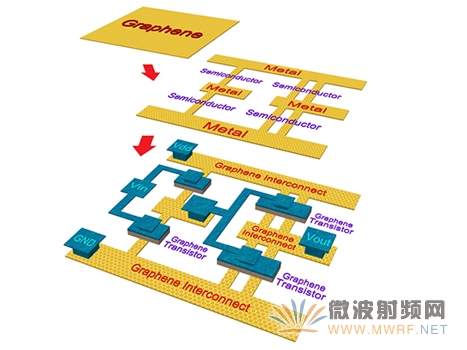
目前,用來制造晶體管和互聯設備的都是大塊材料,因此很難讓集成電路變得更小,而且大塊材料也容易導致晶體管和互聯設備之間的“接觸電阻”變大,而這兩方面都會降低晶體管和互聯設備的性能并增加能耗。基于石墨烯的晶體管和互連設備極具前景,有望解決這些基本問題。
該研究的領導者、加州大學圣巴巴拉分校(UCSB)電子和計算機工程系教授、納米電子設備研究實驗室主任高斯塔夫·巴納吉表示:“石墨烯除了是目前最纖薄的材料之外,其還具有一個可調諧的帶隙。狹窄的石墨烯帶能被用來制造半導體;而寬的石墨烯帶是金屬。不同的石墨烯帶可以制成不同的設備,制成的設備可以無縫地結合在一起,這樣也可以降低接觸電阻。”
在實驗中,巴納吉研究團隊使用非平衡格林函數(NEGF)來對包含有如此多異質結構的復雜電路架構的性能進行評估,并研究出了一種方法,設計出了這種“全石墨烯”的邏輯電路。該研究的合作者康家豪(音譯)表示:“對電子通過由不同類型的石墨烯納米帶制造的設備和互連設備的情況以及跨過其接口的情況進行精確的評估是我們的電路設計成功并達到最優化的關鍵。”
石墨烯研究領域的大咖、哥倫比亞大學的物理學教授菲利普·吉姆表示:“這項研究通過使用一種全石墨烯的設備——互聯架構,為傳統集成電路會遇到的接觸電阻問題提供了一種解決辦法,這將顯著簡化基于石墨烯的納米電子設備的集成電路構建過程。”
結果表明,與目前的集成電路技術相比,新的全石墨烯電路的噪聲容限更高,且耗費的靜態功耗低很多。另外,巴納吉表示,隨著石墨烯研究領域不斷取得進展,這種全石墨烯電路有望在不久的將來成為現實。
原文參考:
Researchers Advance Scheme to Design Seamless Integrated Circuits Etched on Graphene
UC Santa Barbara researchers demonstrate seamless designing of an atomically-thin circuit with transistors and interconnects etched on a monolayer of graphene
Researchers in electrical and computer engineering at UC Santa Barbara have introduced and modeled an integrated circuit design scheme in which transistors and interconnects are monolithically patterned seamlessly on a sheet of graphene, a 2-dimensional plane of carbon atoms. The demonstration offers possibilities for ultra energy-efficient, flexible, and transparent electronics.
Bulk materials commonly used to make CMOS transitors and interconnects pose fundamental challenges in continuous shrinking of their feature-sizes and suffer from increasing "contact resistance" between them, both of which lead to degrading performance and rising energy consumption. Graphene-based transistors and interconnects are a promising nanoscale technology that could potentially address issues of traditional silicon-based transistors and metal interconnects.
"In addition to its atomically thin and pristine surfaces, graphene has a tunable band gap, which can be adjusted by lithographic sketching of patterns - narrow graphene ribbons can be made semiconducting while wider ribbons are metallic. Hence, contiguous graphene ribbons can be envisioned from the same starting material to design both active and passive devices in a seamless fashion and lower interface/contact resistances," explained Kaustav Banerjee, professor of electrical and computer engineering and director of the Nanoelectronics Research Lab at UCSB. Banerjee's research team also includes UCSB researchers Jiahao Kang, Deblina Sarkar and Yasin Khatami. Their work was recently published in the journal Applied Physics Letters.
"Accurate evaluation of electrical transport through the various graphene nanoribbon based devices and interconnects and across their interfaces was key to our successful circuit design and optimization," explained Jiahao Kang, a PhD student in Banerjee's group and a co-author of the study. Banerjee's group pioneered a methodology using the Non-Equilibrium Green's Function (NEGF) technique to evaluate the performance of such complex circuit schemes involving many heterojunctions. This methodology was used in designing an "all-graphene" logic circuit reported in this study.
"This work has demonstrated a solution for the serious contact resistance problem encounterd in conventional semiconductor technology by providing an innovative idea of using an all-graphene device-interconnect scheme. This will significantly simplify the IC fabrication process of graphene based nanoelectronic devices." commented Philip Kim, professor of physics at Columbia University, and a renowned scientist in the graphene world.
As reported in their study, the proposed all-graphene circuits have achieved 1.7X higher noise margins and 1-2 decades lower static power consumption over current CMOS technology. According to Banerjee, with the ongoing worldwide efforts in patterning and doping of graphene, such circuits can be realized in the near future.
"We hope that this work will encourage and inspire other researchers to explore graphene and beyond-graphene emerging 2-dimensional crystals for designing such ‘band-gap engineered' circuits in the near future," added Banerjee.
Their research was supported by the National Science Foundation.
 粵公網安備 44030902003195號